
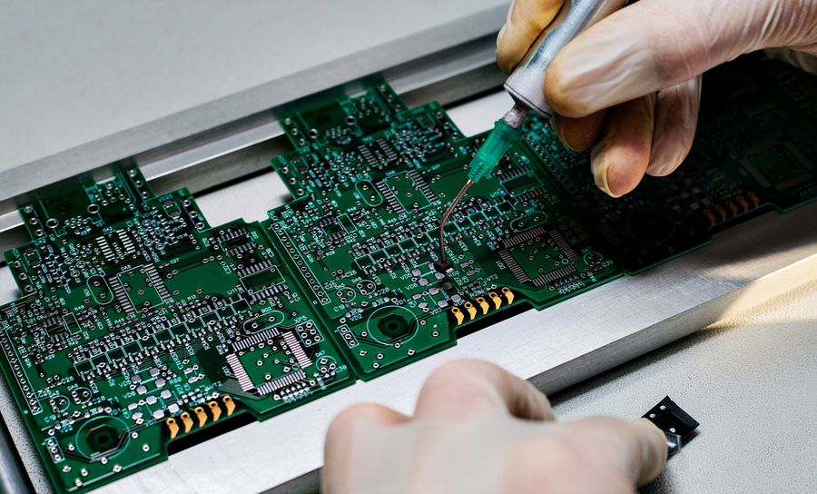
PCB panelization is a manufacturing technique that combines multiple printed circuit boards (PCBs) into a single panel for more efficient fabrication, assembly, handling, and testing. Instead of processing individual boards separately, manufacturers arrange multiple PCB designs or repeated copies of the same design within a larger panel that fits their production equipment and process requirements.
Effective PCB panelization helps manufacturers improve material utilisation, simplify handling, support automated assembly, and maintain consistent production quality. However, the panel layout must account for board dimensions, tooling holes, fiducials, separation methods, manufacturing tolerances, and the risk of damage during depanelization.
For PCB manufacturers, selecting the right panelization method is an important part of CAM engineering and design for manufacturability (DFM). This guide explains common PCB panelization methods, essential design rules, tooling requirements, and manufacturing considerations that influence production efficiency and yield.
What Is PCB Panelization?
PCB panelization is the process of arranging individual circuit boards within a larger manufacturing panel. The panel may contain multiple copies of one PCB design or several different designs, depending on production requirements.
The boards remain connected through temporary structures or are arranged with suitable separation features so that they can be handled and processed as a panel. After the required manufacturing or assembly operations, individual boards are separated using an appropriate depanelization method.
PCB panelization is commonly used in:
- High-volume PCB fabrication.
- Surface-mount technology (SMT) assembly.
- Automated component placement and inspection.
- Production of small or irregularly shaped boards.
- Manufacturing environments that require consistent board handling.
- Projects involving multiple PCB designs in a shared panel.
A well-designed panel must balance manufacturing efficiency with board integrity. Increasing the number of boards per panel is not always the best solution if it creates handling difficulties, increases mechanical stress, or reduces manufacturing yield.
Why PCB Panelization Matters
PCB panelization affects several stages of the manufacturing process, including fabrication, assembly, inspection, handling, and final separation.
A suitable panel layout can help manufacturers:
- Improve utilisation of available panel material.
- Reduce repetitive handling of individual boards.
- Support automated assembly and inspection.
- Maintain consistent positioning during production.
- Improve throughput for small PCB designs.
- Simplify manufacturing and tooling arrangements.
- Reduce unnecessary material waste.
- Minimise damage associated with board handling and separation.
However, poor panelization can introduce problems such as excessive mechanical stress, inadequate tooling space, difficult depanelization, and inconsistent board positioning.
Manufacturers should therefore evaluate panelization alongside the complete manufacturing workflow rather than treating it as an isolated layout task.
Common PCB Panelization Methods
The appropriate panelization method depends on board geometry, material properties, component placement, assembly equipment, production volume, and separation requirements.
1. Step-and-Repeat Panelization
Step-and-repeat panelization places multiple copies of the same PCB design across a manufacturing panel. The design is repeated in a planned arrangement to make efficient use of the available panel area.
This method is commonly used when manufacturers produce large quantities of the same board.
Key considerations include:
- Board spacing and edge clearances.
- Panel dimensions and equipment limitations.
- Consistent board orientation.
- Tooling hole and fiducial placement.
- Manufacturing tolerances.
- Routing or scoring requirements.
Step-and-repeat layouts can improve material utilisation and simplify production planning. The final arrangement should still provide sufficient clearance for fabrication, assembly, inspection, and separation operations.
2. Multi-Design Panelization
Multi-design panelization combines two or more different PCB designs within the same manufacturing panel.
This approach can be useful when a manufacturer needs to process smaller production quantities or coordinate multiple designs with compatible manufacturing requirements.
Important considerations include:
- Different board dimensions and shapes.
- Material and thickness compatibility.
- Component heights and assembly requirements.
- Separation methods for each design.
- Manufacturing priorities and order quantities.
- Traceability and identification of individual designs.
Not every PCB design is suitable for combination within one panel. Manufacturers should verify that the designs share compatible fabrication and assembly requirements before approving a mixed panel.
3. Tab-Routed Panelization
Tab-routed panelization connects individual PCBs to the surrounding panel through small tabs. The tabs hold boards in position during manufacturing and assembly while allowing them to be separated later.
This method is useful for irregularly shaped boards or designs that require additional support during automated handling.
The design should account for:
- Tab locations and dimensions.
- Mechanical strength during assembly.
- Board edge quality after separation.
- Component clearance near tabs.
- Stress on solder joints and sensitive components.
- Accessibility for depanelization equipment.
Breakaway tabs may leave small protrusions or rough edges after separation. Their placement should be selected to minimise interference with components, enclosures, connectors, and final product dimensions.
4. V-Scoring
V-scoring creates V-shaped grooves along designated separation lines between adjacent boards. These grooves reduce the remaining material thickness, allowing the boards to be separated after manufacturing or assembly.
V-scoring is generally most suitable for boards with straight separation edges and compatible panel geometry.
Important design considerations include:
- Straight and aligned board edges.
- Remaining material thickness.
- Board thickness and material characteristics.
- Component clearance near the score line.
- Depanelization equipment and handling.
- Mechanical stress during separation.
Components placed too close to a score line may be exposed to mechanical stress or clearance problems. Manufacturers should follow their fabricator's requirements for score geometry and component placement.
V-scoring is not appropriate for every board shape. Irregular outlines, curved edges, and complex internal features may require routing or another separation approach.
5. Routed Panelization
Routed panelization uses a routing tool to cut the board outline or create separation paths between adjacent PCBs. Small connecting tabs may be retained where needed to hold boards together.
Routing supports complex shapes and can provide greater flexibility than V-scoring for irregular board outlines.
Considerations include:
- Routing path and tool diameter.
- Minimum spacing between adjacent boards.
- Tab placement and quantity.
- Edge quality requirements.
- Material utilisation.
- Mechanical stress during separation.
- Access for routing tools.
Routing can offer flexibility for designs that cannot use straight score lines. However, routing paths and clearance requirements may increase material usage or affect the number of boards that fit within a panel.
Essential PCB Panelization Design Rules
PCB panelization design rules help ensure that the panel can be manufactured, assembled, inspected, and separated reliably. Exact requirements depend on the fabricator, board design, material, production equipment, and assembly process.
Manufacturers should confirm their specific requirements before finalising a panel layout.
1. Panel Dimensions and Board Spacing
Panel dimensions must fit the manufacturer's fabrication and assembly equipment. The layout should also provide adequate space between boards and around the panel edges.
Insufficient spacing can interfere with routing, scoring, tooling, or automated assembly.
When determining board placement, consider:
- Maximum and minimum panel dimensions.
- Required spacing between PCB outlines.
- Available fabrication area.
- Assembly equipment limitations.
- Routing tool clearance.
- Edge clearance for tooling and handling.
Board spacing should be based on the intended separation method and the manufacturer's process capabilities rather than an assumed universal value.
2. Tooling Holes
Tooling holes are used to position and align panels during manufacturing and assembly. They help establish consistent references for equipment that holds, locates, or processes the panel.
Depending on the workflow, tooling holes may support panel registration, assembly fixtures, or mechanical alignment.
When planning tooling holes, consider:
- Hole diameter and positional tolerance.
- Distance from the panel edge.
- Compatibility with fixtures and equipment.
- Clearance from electrical features.
- Consistency across panel revisions.
- Whether the holes are intended for the panel or individual boards.
Tooling holes should be placed according to the fabricator's specifications and the requirements of downstream assembly equipment.
3. Fiducial Marks
Fiducials are visual reference marks used by automated optical systems to determine PCB or panel position and orientation. They are especially important in SMT assembly, where machines use optical recognition to align component placement accurately.
Fiducials may be provided at the panel level, board level, or both, depending on the assembly process.
Important considerations include:
- Fiducial size and shape.
- Copper and solder mask clearance.
- Visibility to machine vision systems.
- Placement relative to the board and panel.
- Avoiding nearby markings or features that interfere with recognition.
- Compatibility with assembly equipment requirements.
Global fiducials help identify the panel's overall position, while local fiducials can provide additional references for individual boards or fine-pitch components.
The required number, dimensions, and placement of fiducials should be confirmed with the assembly provider.
4. Panel Rails
Panel rails are additional strips of material attached to the sides of a PCB panel. They provide space for handling, tooling holes, fiducials, and other manufacturing references.
Rails can help automated assembly equipment grip and transport panels that would otherwise be too small or difficult to handle.
When designing panel rails, consider:
- The width required by the assembly equipment.
- Tooling hole and fiducial placement.
- Conveyor support requirements.
- Board-edge clearance.
- Rail removal after assembly.
- Additional material usage.
- Mechanical stability during processing.
Not every panel requires rails. Their use depends on board dimensions, assembly equipment, handling requirements, and the manufacturer's production process.
5. Component-to-Edge Clearance
Components located near board edges may be vulnerable to mechanical stress during routing, scoring, or breakaway-tab separation.
Panelization should provide sufficient clearance between components and the intended separation lines.
Pay particular attention to:
- Large or heavy components.
- Connectors extending toward the board edge.
- Fine-pitch components.
- Brittle or mechanically sensitive parts.
- Components with solder joints close to separation features.
- Components that could obstruct routing or scoring tools.
Clearance requirements depend on component design, board thickness, separation equipment, and assembly conditions. The assembly provider's guidelines should be used when establishing final placement rules.
6. Board Orientation and Assembly Direction
Board orientation can influence component placement, assembly throughput, and handling efficiency.
Arranging boards consistently may simplify automated processing, but the best orientation depends on component layout, conveyor direction, tooling constraints, and manufacturing equipment.
During panel planning, evaluate:
- Assembly line direction.
- Component orientation requirements.
- Placement machine access.
- Inspection accessibility.
- Panel balance and stability.
- Separation direction and handling.
A layout that maximises the number of boards may not provide the most efficient assembly configuration. Both material utilisation and production performance should be considered.
Manufacturing Considerations That Influence Panelization
Material Utilisation
Material utilisation measures how efficiently the available panel area is used for PCB production.
A panel layout with less unused space can reduce material waste. However, board spacing, routing clearance, panel rails, tooling features, and handling requirements all consume space.
The goal is to achieve a practical balance between the number of boards per panel and the requirements of the manufacturing process.
Manufacturers should compare alternative layouts using actual panel dimensions, separation methods, and production constraints.
Depanelization and Mechanical Stress
Depanelization is the process of separating individual PCBs from a manufacturing panel. The separation method can influence edge quality, board stress, component reliability, and the amount of post-processing required.
Routing, V-scoring, and tab-based separation each have different mechanical characteristics.
For sensitive designs, manufacturers should evaluate whether separation forces could damage solder joints, components, or the board itself. Appropriate tab placement, clearance planning, and depanelization equipment can help reduce these risks.
Manufacturing Equipment Compatibility
Panelization must match the requirements of the equipment used throughout fabrication and assembly.
This includes panel handling, automated optical inspection, SMT placement, soldering, routing, and testing equipment.
Before approving a panel design, confirm:
- Permitted panel dimensions.
- Conveyor and fixture requirements.
- Tooling hole specifications.
- Fiducial requirements.
- Rail requirements.
- Separation equipment compatibility.
- Any customer-specific panel standards.
Coordination between CAM engineering, fabrication, and assembly teams helps prevent avoidable production issues.
Traceability and Board Identification
Panels containing multiple PCB designs or customer orders require appropriate identification and traceability.
Design references, panel identifiers, revision information, and manufacturing records should remain consistent throughout the production process.
The identification method must not interfere with electrical features, component placement, tooling, or separation.
For multi-design panels, manufacturers should also define how individual boards will be identified after depanelization.
How PCB Panelization Affects Manufacturing Yield
Manufacturing yield refers to the proportion of manufactured units that meet the defined acceptance criteria. PCB panelization can influence yield through material utilisation, mechanical handling, alignment, assembly consistency, and separation quality.
An efficient panel layout does not automatically produce a higher yield. The layout must also support reliable processing and avoid introducing unnecessary risks.
Factors That Can Reduce Yield
Poor panel layout: Inadequate spacing or unsuitable board orientation can create manufacturing and handling difficulties.
Incorrect tooling placement: Misaligned or incompatible tooling features can affect panel positioning during fabrication or assembly.
Inadequate fiducial design: Poor visibility or unsuitable placement may interfere with automated optical alignment.
Improper separation design: Poorly positioned tabs or unsuitable scoring lines can increase mechanical stress and damage risk.
Component placement near edges: Components located too close to separation features may experience stress during depanelization.
Insufficient design validation: Failure to check the panel against manufacturing rules can lead to issues that are expensive to correct after production begins.
How to Improve Panelization Yield
Manufacturers can improve panelization reliability by:
- Applying documented DFM checks before panel release.
- Confirming tooling and fiducial requirements with assembly teams.
- Selecting separation methods that suit the board design.
- Reviewing component clearances near panel edges.
- Verifying panel dimensions and manufacturing tolerances.
- Testing new panel layouts before high-volume production.
- Tracking defects associated with handling and depanelization.
- Updating panelization rules based on production feedback.
Monitoring yield by design, panel configuration, and separation method can help manufacturers identify recurring problems and refine their panelization practices.
The Role of CAM Engineering in PCB Panelization
CAM engineering connects PCB design data with manufacturing requirements. During panelization, CAM engineers review board geometry, manufacturing files, spacing requirements, tooling features, and separation methods to prepare a suitable production layout.
A typical workflow includes:
- Reviewing the supplied PCB design files and fabrication requirements.
- Checking board outlines, dimensions, and manufacturing constraints.
- Selecting a suitable panelization approach.
- Arranging boards according to panel and equipment limits.
- Adding required tooling holes, fiducials, and panel rails.
- Defining routing paths, tabs, or V-scoring features.
- Checking clearances and manufacturing data.
- Verifying the final panel layout before production release.
Effective PCB CAM engineering services can support this process by helping manufacturers validate design data, prepare tooling outputs, and identify potential manufacturing issues before fabrication.
Front-end processing and DFM checks are also important because panelization decisions depend on accurate board outlines, complete manufacturing files, and a clear understanding of production requirements. Learn more about PCB front-end engineering services.
PCB Panelization Checklist Before Manufacturing
Use this checklist when reviewing a PCB panel layout before production release.
- Confirm panel dimensions comply with fabricator requirements.
- Verify board spacing and edge clearances.
- Confirm the selected panelization method suits the board geometry.
- Check tooling hole locations and dimensions.
- Verify fiducial placement and visibility.
- Confirm whether panel rails are required.
- Check component clearance around routing and scoring lines.
- Review tab placement and mechanical support.
- Verify routing paths or V-scoring requirements.
- Confirm compatibility with assembly and inspection equipment.
- Check panel identification and revision information.
- Validate the final panel data before production release.
This checklist should be adapted to the fabricator's process specifications and the requirements of the assembly provider.
Common PCB Panelization Mistakes to Avoid
Selecting a Method Based Only on Board Count
Maximising the number of boards per panel may appear cost-effective, but an overly dense layout can create problems with tooling, routing, assembly, or depanelization.
Evaluate total manufacturing performance rather than board count alone.
Ignoring Assembly Requirements
A panel designed only for PCB fabrication may not work efficiently on the assembly line.
Include the assembly provider's requirements for rails, fiducials, board orientation, and panel handling before finalising the layout.
Placing Components Too Close to Separation Features
Insufficient clearance around V-scores, routing paths, or breakaway tabs can increase the risk of component damage.
Review sensitive components and mechanical constraints during the panelization stage.
Using Inconsistent Tooling and Fiducial Locations
Inconsistent references can complicate panel alignment and automated assembly.
Follow documented manufacturing and assembly standards, and ensure that tooling features remain consistent across approved revisions.
Skipping Final CAM Validation
Panelization changes board arrangements and introduces additional manufacturing features. The final output should be reviewed to confirm that dimensions, spacing, tooling, separation paths, and revision details are correct.
Conclusion
PCB panelization is an important part of PCB manufacturing because it influences material utilisation, production efficiency, assembly handling, separation quality, and manufacturing yield.
Step-and-repeat layouts, multi-design panels, tab routing, and V-scoring each offer different advantages. The right method depends on board geometry, production volume, component placement, equipment compatibility, and the required separation process.
A reliable panelization workflow should include accurate tooling holes, suitable fiducials, appropriate panel rails where required, adequate component clearances, and final CAM validation. Manufacturers should also coordinate with assembly teams and monitor production results to identify opportunities for improvement.
For PCB manufacturers looking to improve panel preparation and manufacturing data quality, explore Goalsr's engineering services or contact the team to discuss your requirements.